Parallel Input Serial Output Shift Register Verilog Code
Parallel-in/ serial-out shift registers do everything that the previous serial-in/ serial-out shift registers do plus input data to all stages simultaneously. The parallel-in/ serial-out shift register stores data, shifts it on a clock by clock basis, and delays it by the number of stages times the clock period. In addition, parallel-in/ serial-out really means that we can load data in parallel into all stages before any shifting ever begins.
This is a way to convert data from a parallel format to a serial format. By parallel format we mean that the data bits are present simultaneously on individual wires, one for each data bit as shown below. By serial format we mean that the data bits are presented sequentially in time on a single wire or circuit as in the case of the “data out” on the block diagram below. Cargo optimizer license key.
SI is Serial Input. PO is Parallel Output. Verilog fpga gpio. (Verilog code) to recreate the. Use of an unitialized register. Design of Parallel In - Serial OUT Shift Register using. Output dout; input. How to write verilog code for 16 bit 2's complement serial.
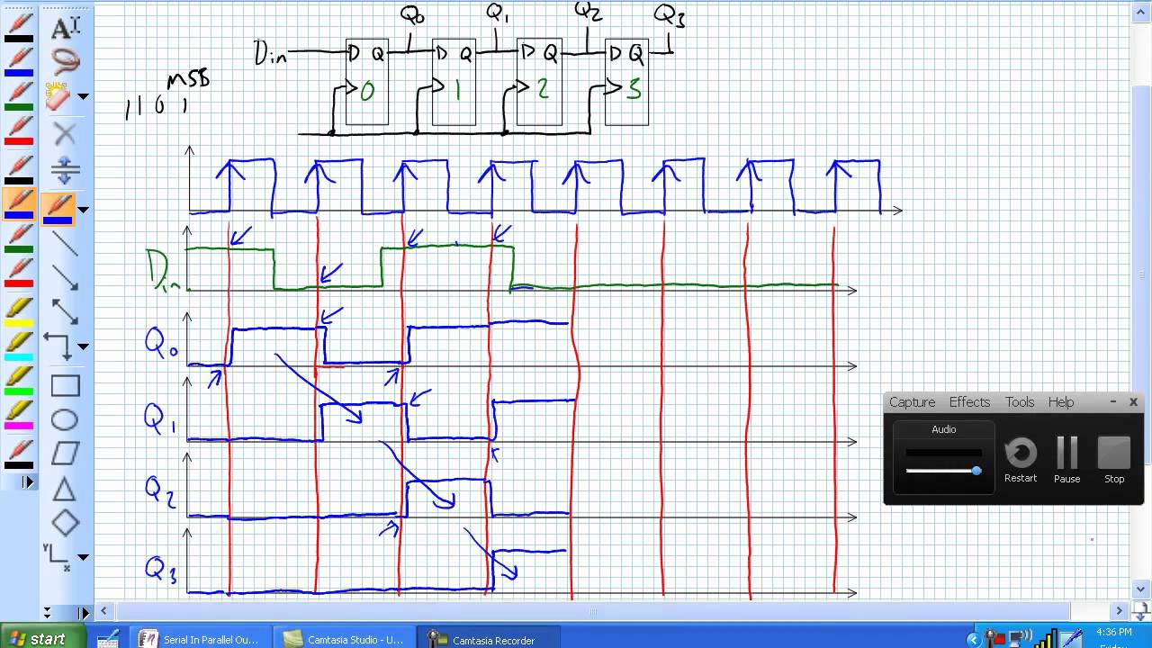
Below we take a close look at the internal details of a 3-stage parallel-in/ serial-out shift register. A stage consists of a type for storage, and an AND-OR selector to determine whether data will load in parallel, or shift stored data to the right. In general, these elements will be replicated for the number of stages required. We show three stages due to space limitations. Four, eight or sixteen bits is normal for real parts. Above we show the parallel load path when SHIFT/LD’ is logic low. The upper NAND gates serving D A D B D C are enabled, passing data to the D inputs of type D Flip-Flops Q A Q B D C respectively.
At the next positive going clock edge, the data will be clocked from D to Q of the three FFs. Three bits of data will load into Q A Q B D C at the same time. The type of parallel load just described, where the data loads on a clock pulse is known as synchronous load because the loading of data is synchronized to the clock. This needs to be differentiated from asynchronous load where loading is controlled by the preset and clear pins of the Flip-Flops which does not require the clock. Only one of these load methods is used within an individual device, the synchronous load being more common in newer devices. The shift path is shown above when SHIFT/LD’ is logic high.
The lower of the pairs feeding the are enabled giving us a shift register connection of SI to D A, Q A to D B, Q B to D C, Q C to SO. Clock pulses will cause data to be right shifted out to SO on successive pulses. The waveforms below show both parallel loading of three bits of data and serial shifting of this data. Parallel data at D A D B D C is converted to serial data at SO. What we previously described with words for parallel loading and shifting is now set down as waveforms above.
As an example we present 101 to the parallel inputs D AA D BB D CC. Next, the SHIFT/LD’ goes low enabling loading of data as opposed to shifting of data. It needs to be low a short time before and after the clock pulse due to setup and hold requirements. It is considerably wider than it has to be. Though, with synchronous logic it is convenient to make it wide.
We could have made the active low SHIFT/LD’ almost two clocks wide, low almost a clock before t 1 and back high just before t 3. The important factor is that it needs to be low around clock time t 1 to enable parallel loading of the data by the clock.
Note that at t 1 the data 101 at D A D B D C is clocked from D to Q of the Flip-Flops as shown at Q A Q B Q C at time t 1. This is the parallel loading of the data synchronous with the clock. Now that the data is loaded, we may shift it provided that SHIFT/LD’ is high to enable shifting, which it is prior to t 2. At t 2 the data 0 at Q C is shifted out of SO which is the same as the Q C waveform. It is either shifted into another integrated circuit, or lost if there is nothing connected to SO. The data at Q B, a 0 is shifted to Q C. The 1 at Q A is shifted into Q B.
With “data in” a 0, Q A becomes 0. After t 2, Q A Q B Q C = 010. After t 3, Q A Q B Q C = 001. This 1, which was originally present at Q A after t 1, is now present at SO and Q C. The last data bit is shifted out to an external integrated circuit if it exists.
Free Download Babul Supriyo Sochta Hun Uska Dil MP3, Size. Free Sochta Hoon Uska Dil Kabhi Mujhpe Aaye Toh Wmv mp3. Matiagi Song Mp3 Mp3.